LED manufacturers reduce cost with automation, larger wafers, new materials (MAGAZINE)
+++++
This article was published in the March 2012 issue of LEDs Magazine.
View the Table of Contents and download the PDF file of the complete March 2012 issue, or view the E-zine version in your browser.
+++++
The LED Manufacturing track at Strategies in Light 2012 featured several speakers who primarily focused on cost-reduction methods in LED manufacturing. Topics included the importance of moving to larger-diameter wafers to the use of materials that can withstand higher-temperature LED operation.
Iain Black, VP of manufacturing engineering and innovation at Philips Lumileds, provided the first of two keynote talks. He stated that the complexity of LED products and applications and the diverse array of customers in the illumination market make low-cost LED manufacturing a tremendous challenge. “There are numerous applications and thousands of LEDs that need to be matched together,” he said.
Black continued, “We still will have custom solutions in cases of very large customers or niche products, but the practice of customizing single-die emitters for lighting is no longer practical.” In addition, the company is building highly-configurable manufacturing lines to achieve the necessary flexibility. Lumileds is in the process of expanding its LED back-end assembly facility in Penang, Malaysia. The all-LED-lit facility is aimed at completion in mid-2012.
LED manufacturing supply and demand
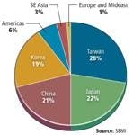
The changing global landscape of LED manufacturing was discussed by Karen Savala, president of SEMI America. SEMI has estimated that there are 142 LED fabs in operation worldwide, up from 64 facilities in 2006. Capacity in 2012 is estimated at 1.57 million (4-inch-equivalent) wafers per month, with the global distribution shown in Fig. 1. Taiwan has the greatest LED chip-manufacturing capacity, followed by Japan and China.
Savala commented that some of the recent build-up in China has been put on hold due to falling LED prices and oversupply concerns. “We see some overcapacity, but we believe this will be a short-term issue,” she said. Savala also provided an update of sapphire substrate prices, which had fallen to a new low of $10 per 2-inch substrate by the end of 2011 (Fig. 2).
Manufacturing roadmap on schedule
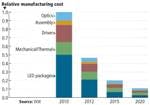
Jim Brodrick, the US DOE’s solid-state lighting program manager, began his talk by inviting the audience to download the Manufacturing Roadmap for Solid-state Lighting Research & Development (www.ssl.energy.gov/techroadmaps.html) and to actively participate in its on-going revision. He stated that the industry is essentially on schedule with the roadmap to achieve LED efficacy of 176 lm/W in 2012 with a price of $6/klm (cool white). Brodrick cited two priorities in the roadmap, which are the development of flexible and cost-effective manufacturing methods for LED modules, light engines and luminaires as well as high-speed, non-destructive test equipment and standardized test procedures for key stages in the manufacturing process. For LED luminaires, a 20× reduction in manufacturing cost is projected between 2010 and 2020 (Fig. 3).
Brodrick emphasized that cost reduction, while maintaining high-quality manufacturing, all comes down to one metric: binning yield. The DOE is funding programs in upstream process control, non-destructive testing, manufacturing automation, and advanced packaging schemes that can lead to higher binning yields. In packaging, Brodrick said that higher levels of component integration are needed, and that LED companies will in general move to wafer-scale packaging for cost reasons.
He noted that of the DOE’s total SSL program, worth $114 million in 2011, 31% is dedicated to OLED-related activities. The roadmap calls for a reduction in OLED luminaire manufacturing cost from around $230/klm in 2012 to under $20/klm in 2020. “High-speed, low-cost, thin-film deposition for OLED production probably will require new tool platforms,” said Brodrick. He added that developments in large-screen OLED-based displays, including large-scale deposition methods and automation, should benefit the OLED lighting market. Some of the focus areas for cost reduction include better utilization of materials, reduced organic layer cost and improved encapsulation methods.
Wafer size increases
Jacob Tarn, president of TSMC Solid State Lighting Ltd, presented a talk entitled “Can a major semiconductor player accelerate the LED cost-reduction curve?” TSMC is the world’s largest semiconductor foundry company. He answered his own question in the affirmative, stating that many high-productivity processes can be transferred from semiconductor to LED manufacturing.
Firstly, he said, there is a need for an integrated development environment in LED manufacturing that includes device and process simulation, similar to what exists in semiconductor manufacturing. “The GaN industry has not had enough databases to build the infrastructure, so many developments have been empirical,” he stated.
TSMC plans to bring fully automated 8-inch manufacturing processes to LED manufacturing. For instance, Tarn talked about growing epilayers on 4-inch or 6-inch substrates, then transferring the GaN-based epilayers to 8-inch wafers using wafer bonding. Then, final processing – including metallization, passivation, phosphor coating and lens molding – can be performed, followed by wafer dicing and testing. In terms of process and equipment control, mainstays of the semiconductor process control world, including run-to-run control, data mining and equipment tracking, can be applied to LED manufacturing.
Beyond these steps, Tarn suggested that perhaps optics can be developed for multiple LED emitters, and that control functions might be integrated at the LED chip or package level.
Raja Parvez, CEO of Rubicon Technology, then talked about the advantages of progressing to larger-diameter sapphire substrates as well as recent industry trends. He said that there are essentially five major producers of sapphire wafers, who all added capacity in the last year, leading to significant price reduction. However, he contends that few manufacturers can provide high-quality large-diameter substrate material and that at the wafer level, flatness and defect-free manufacturing are much more difficult to achieve.
Improved wafer flatness has been correlated with more consistent lithographic results and greater consistency in brightness and color of LEDs. To date, Rubicon has shipped over 230,000 6-inch polished sapphire wafers.
Tool productivity
Thomas Uhrmann of EV Group cited lithographic patterning as a key cost-reduction area for LED manufacturers. Some of the parameters that affect patterning yield include warpage and poor visibility of alignment marks due to the light-scattering properties of LED wafers. In this area, 1× steppers compete with proximity aligners.
Many LED manufacturers are now pursing vertical LED structures, which may be capable of higher light-extraction efficiency than lateral designs, while providing good heat conduction to the submount assembly or package, according to Uhrmann. For these structures, EV Group has developed a variety of eutectic bonding and transient liquid-phase bonding processes capable of withstanding high temperature cycling in the latter process steps.
Defect and yield management
Abdul Lateef, CEO of Plasma-Therm, a maker of plasma-enhanced CVD (PECVD) tools, discussed the demand for better data management from LED manufacturers. He provided an example of how in-situ metrology is helping to automate the process. “We have equipped our PECVD tools with optical emission interferometry which uses the light from the plasma to monitor film thickness,” he said.
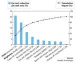
Mike Plisinski of Rudolph Technologies also discussed the theme of metrology and yield management methods. He said “Epi engineers have little visibility into the impact of epi on downstream LED processes.” Plisinski suggested a concentration of process-control resources at the epitaxial process level. Fig. 4 shows that LED yield and light output have the greatest impact on overall epi cost reduction.
Next, Dan Scharpf of Labsphere talked about optical testing of LEDs. He said that one of the challenges in LED manufacturing is identifying which process steps impart the greatest variation in lumen output and color of the LED. He also said that more LED manufacturers are interested in performing LED testing at elevated temperatures. He stated that thermal control is a challenge, whether the test is performed at the wafer, die or module level. Scharpf added that testing at elevated temperatures will increase test times because an equilibrium condition must be achieved. He further warned that if an LED undergoes self-heating, operating wavelength is likely to shift and measured flux can change significantly.
Thermal management
Geoff Gardner of Dow Corning talked about innovations in silicone technology as applied to LEDs. Silicone is perhaps best known for its use as an LED chip encapsulant. Garner said the company has developed silicone with a higher refractive index specifically for high-power LEDs. “Any LED above 0.5 watt is going to require a higher-refractive-index material capable of withstanding high operating temperatures,” he said.
Silicone is also used for injection-molded secondary optics such as total-internal-reflection lenses. In the case of remote-phosphor optics, silicone can withstand higher temperatures than the prevailing material used today, a polycarbonate. Finally, thermal-interface materials made of silicone can be screen printed and cut to virtually any shape to provide stress relief, shock dampening and/or heat transfer in a variety of LED lamp and luminaire applications.
Packaging cost
Ilkan Cokgor of Everlight Electronics focused his talk on processes for plastic leaded chip carrier (PLCC) packages. PLCCs are low-cost surface-mount packages that have not developed a reputation for reliability in LED packaging until recently. These packages distribute heat and light through spatially distributed LEDs.
Cokgor pointed to several recent improvements in PLCC packages. These include a modified primary optic; a new alloy nitridation process that improves the crystal structure of the phosphor material and improves brightness; and new sidewall etching and patterned-sapphire-substrate processes on the chips. The PLCC also uses a die-attach material with higher thermal conductivity (0.8 W/mK) and a higher efficiency reflector.
Ravi Bhatkal of Cookson Electronics discussed some of the thermal challenges associated with using package, submount and board materials that all have different coefficients of thermal expansion. Fast temperature changes induce more thermal stress and can lead to creep failures. He suggested a combination of relevant material stack design, thermal modeling and advanced thermal cycling tests to provide a mapping function between accelerated test results and estimated useful lifetime.


