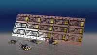
Date Announced: 21 Feb 2010 The new stamped circuit board (SCB) technology available from Heraeus opens up a whole new concept of thermal management geared towards the realization of reliable and economic solutions in the area of thermal dissipation. The demands placed on electronic systems are continually growing, whilst the systems themselves are become ever smaller and increasingly complex. Heraeus‘ reaction to this ongoing trend towards miniaturization has been to develop a sophisticated smart solution. The SCB technology is specially designed for small circuits. Its use means that various differing metal/ plastic combinations can be structured and laminated in their millions in an extremely efficient manufacturing process. Heraeus sets the standard worldwide in microelectronics For many years now stamped metal substrates made by Heraeus have been widely used as component carriers in the electronic branch. Based on this experience, the SCB technology goes a step further and combines structured metal layers with layers of likewise structured plastic. Similar to printed circuit boards, this multilayer structure may comprise glass fiber reinforced epoxy resin and copper. However, the separate structuring of the two materials allows for completely new design concepts. The manufacturing process in itself is also quite different. For a start the plastic and the metal are processed on separate reels. In accordance to the corresponding requirements the materials are structured whilst being stamped and then subsequently joined together in a perfect fit during lamination. If a special surface is needed for future specific applications then this is possible through electroforming. All of the production stages run in a highly efficient reel to‐ reel process. Expertise in materials, surface technology and tooling – and all from a single source Leading lighting manufacturers profit considerably from this new technology as regards their LED products. Luminous flux, efficiency and lifespan of LEDs depend to a large extent on their own junction temperature. Thus, any increase in the component temperature will have a negative effect on the performance of the LED. As such, it is obvious that an ingeniously devised thermal management system is something of tremendous significance. The SCB technology, as chip carrier, makes a decisive contribution towards the electrical and thermal properties and assumes a key role in the deployment of a wide variety of thermally conductive metals respectively metal alloys. The advantages of SCB technology are apparent: SCB is the optimal circuit board technology for small‐circuitry design. The highprecision stamping is ideally suited to the manufacture of small structures in the range of bridge and slot widths up to 60 μm in 40 μm thin materials as well as for mass production. These strengths of material enable low package heights and provide in addition the advantage of being considerably more flexible. As opposed to the more classical printed circuit board, SCB offers the means to simply structure the layer of plastic and so create new possibilities for contacting. The components can be directly placed on top of the existing metal layer using a conductive adhesive and contacted along the backside of the metal. This means that in the case of temperature‐sensitive components a whole new form of thermal management is created, whereby the thermal energy can be directly dissipated through the conductive copper layer. As a result the inexpensive SCB mass production process means that modular superstructures can be achieved which are capable of producing overall heat conducting values comparable to those of ceramic respectively plastic injection molded superstructures.
Contact
Tom Grunwaldt Marketing & Communication Services W. C. Heraeus GmbH Heraeusstraße 12‐14 63450 Hanau, Germany Phone: + 49 (0) 6181.35‐5433 Fax: + 49 (0) 6181.35‐3131 E‐Mail: [email protected]
E-mail:[email protected]
Web Site:www.heraeus.com


