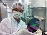
Bridgelux hits 160 lm/W in lab with LEDs produced using GaN on silicon
Bridgelux announced that it has fabricated LEDs in the lab using gallium-nitride-on-silicon (GaN-on-Si) technology that delivers 160 lm/W (cool white) and 125 lm/W (warm white) efficacy.
The performance realized using 8-in wafers is similar to the best efficacy demonstrated in the lab by leading LED vendors using traditional sapphire or silicon carbide wafers, and Bridgelux believes the GaN-on-Si approach will ultimately yield a "75% improvement in cost" for LED components that will in turn reduce the cost of solid-state-lighting (SSL) lamps and luminaires.
The new LEDs deliver a cool-white CCT of 4350K and a warm white CCT of 2940K. The warm white devices have a CRI of 80. The company said that its 1.5-mm blue LEDs can deliver wall-plug efficiency as high as 59% at 350 mA – and says that exceeds any published values from other vendors. The company also claims waveform uniformity of sigma 6.8 nm with a median wavelength of 455 nm.
Getting from the lab to production
Of course the Bridgelux announcement is focused on lab prototypes and production is perhaps two years away. Still it shows progress. Back in March, the company announced the demonstration of 135 lm/W LEDs. Since, the company was able to both boost efficacy considerably and demonstrate that performance on 8-in substrates that are, in large part, a key to lower-cost components.
Bridgelux VP of global marketing Jason Posselt said, "It's important that we demonstrated this on an 8-in wafer." Posselt also believes that Bridgelux has largely closed the performance gap relative to sapphire-based LEDs. Bridgelux's silicon-based LEDs appeared to be 12 to 18 months behind state-of-the-art LEDs in terms of efficacy at the public launch of the company's GaN-on-Si program.
But Posselt acknowledged the challenge that remains in terms of commercializing the technology. The company is building wafers that yield as many as a thousand good die now and ultimately they need to produce 20,000 good die on an 8-in wafer.
Silicon cost advantages
The allure of silicon-based LEDs is purely cost and the savings come in two primary areas. First, the semiconductor industry has the proven ability to manufacture low-cost large silicon wafers. Silicon would both lower baseline wafer cost and pave a smoother transition to larger wafer sizes. Long Yang, vice president of chip technology at Bridgelux, noted that you can get the equivalent number of LEDs from 3 8-in silicon wafers that you get from 42 2-in sapphire wafers today.
The second set of savings come in the back-end of the manufacturing process where fully-depreciated, and fully-automated silicon fabs stand ready to fabricate LEDs. Posselt said "Typical LED fabs are very labor intensive, and not automated like silicon fabs." And those automated fabs are ready to handle 8-in wafers and the far greater number of die on those wafers.
Of course there are technical challenges that stand in the way of a silicon transition as well as skeptics of the economic story. In an informal poll of people at the recent Semicon trade show, many pointed out that a move to silicon doesn't impact the most-expensive part of an LED factory – the MOCVD reactor. Bridgelux's Yang said that the MOCVD reactor represents 40% of the capital expenditure in an LED fab line. He believes there is substantial savings to be had in utilizing automated semiconductor systems for the remainder of the manufacturing process.
Challenges to silicon wafers
Among the challenges to GaN-on-Si technology is the thermal mismatch between the silicon wafer and the GaN layers. That mismatch can lead to cracking in the GaN layers and bowed wafers either during the epitaxial growth process or later at room temperature. Bridgelux says it has solved that problem with a proprietary buffer layer that delivers crack-free "virtually flat" 8-in wafers.
When asked about the remaining challenges, Long mentioned two important milestones and a significant challenge. Yang said, "We need to convert our process to be fully 8-in compatible." He said that Bridgelux is well along in that effort and would complete it soon. The second milestone will be achieving better uniformity across the wafer in the MOCVD reactor, followed by large runs of wafers in pilot production."
Transferable recipe
Long sees the primary challenge as developing a transferable process or recipe. He noted that even the same model of MOCVD reactor have inherent differences. And Bridgelux must develop a recipe that first is usable across the same MOCVD model and subsequently to different reactor models from the same vendor and later to reactors from different vendors. But the company could go into production once it can reliably transfer the process across the same model MOCVD reactor from a single vendor. Bridgelux is working with a single unnamed MOCVD reactor vendor for now.
Assuming, Bridgelux overcomes the technical hurdles, Yang sees other advantages in the GaN-on-Si technology. He said "It's easier to control variations when you load wafers into equipment with robots." Basically he is saying that robotics will yield more consistent components and better yield. Certainly LED manufacturing on sapphire and silicon carbide is evolving toward more automated processes, but that takes time and money.
Meanwhile those silicon fabs stand ready and Bridgelux hopes to partner with a company that can bring expertise in silicon-manufacturing to the table. Posselt asked, "How to we bridge the gap between the opto LED and the semiconductor space?" Presumbaly the answer is a partner that for now is either unidentified or unnamed.
Bridgelux CTO Steve Lester is clearly confident in the progress. He said, "We are very pleased with the pace of our progress in this area, and we will continue to aggressively develop our GaN-on-Si processes in order to drive the migration of LED commercial production from sapphire to silicon substrates. Our first commercially available GaN-on-Si products remain on schedule for delivery to the market within the next two years."


