Patterned substrates enhance LED light extraction (MAGAZINE)
DONGGEUN KO, JACOB YOON, and JANGHO SEO describe how patterned wafers can help increase LED light extraction by reducing defect density and total internal reflection losses.
Manufacturers are quickly adopting nitride-semiconductor-based LEDs as a standard light source for a wide range of products from general lighting, automobile headlights, and traffic signals to backlighting for consumer devices like HDTVs, smartphones, and tablets, and displays large and small. Still, LED performance and cost are gating broad deployment of LED technology. Indeed, lower component pricing and greater light output could boost consumer market acceptance. LED chip manufacturers are looking to patterned sapphire-substrate manufacturing techniques to maximize light extraction and overcome obstacles to broader LED usage.
Patterns applied on an LED substrate or wafer can significantly increase the light output of LEDs in two ways. The technique can increase the light emission of active quantum well layers as the result of reduced epitaxial defect density. And patterned sapphire substrates can reduce light loss due to total internal reflection (TIR) phenomena by enabling a photon scattering effect.
Researchers have developed ways to create patterns — periodic structures of varying geometry and dimension — on the sapphire substrate surface. These sapphire wafers with periodic structures of various shapes such as cone, dome, pyramid, and pillar, etc., are called patterned sapphire substrates (PSS).
There are two different manufacturing processes to fabricate PSS currently being practiced in the industry: dry plasma etching and wet chemical etching. Today, the majority of PSS products are produced by dry plasma etching due to its inherently effective control of precision and uniformity. The discussion of PSS fabrication in this article will focus on inductively coupled plasma (ICP) dry reactive etching (RIE).
Through work on 100-mm and 150-mm PSS with more than a dozen of the most advanced LED manufacturers, Rubicon has a unique opportunity to understand the range of requirements for effective PSS. The most critical requirements are pattern dimension, shape, and aspect ratio (i.e., feature height against width), and uniformity across the wafer as well as consistency from wafer to wafer.
There is no single best universal PSS recipe due to the high degree of customization of the epitaxy processes in the LED industry. Designs for patterning vary widely, and there is no convergence of PSS designs on the horizon. Typical pattern shapes include cones, domes, and square or trigonal pyramids. Although academic studies demonstrate that smaller pattern dimensions (100–1000 nm) provide greater luminous efficiency, the LED industry norm today is still 3- or 4-μm feature size.
Key process parameters contributing to these critical characteristics are the dimensional accuracy and uniformity of photoresist (PR) mask, sapphire etching selectivity against the PR mask, bias RF power, ICP process pressure, RF coil design for plasma uniformity, the ratio of trifluoromethane (CHF3) and boron trichloride (BCl3) gases, and substrate temperature.
Enhanced light extraction
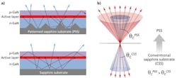
Low light-extraction efficiency is a serious challenge for building high-brightness LEDs. Patterning on the substrate scatters a large number of photons emitted outside the TIR escape cone back into the cone, which helps more light to be extracted (Fig. 1a), creating an effect equivalent to increasing the critical angle of the escape cone (Fig. 1b). As a result, light extraction efficiency has been found to increase by as much as 30%.
Photons are emitted from the active quantum well layers by electron-hole recombination, and they escape the LED die into free space. In an ideal situation, all of the photons emitted by the active layers would be extracted as light output in LEDs. In reality, a large number of the emitted photons never escape the LED die for various reasons.
One key obstacle to such ideal light extraction is TIR effects due to the high refractive index of gallium nitride (GaN) versus the refractive index of free space (about 2.5 to 1.0). A large number of photons generated from the active region bounce back into the die and get trapped inside, eventually dissipating as heat. In terms of the light escape cone, defined by the critical angle of TIR, only light emitted into the escape cone exits the LED die while light emitted outside the cone gets trapped inside.
More effective luminous conversion
In terms of thermal, mechanical, and chemical properties, sapphire is an excellent substrate for III/V chemical-element nitride epitaxial growth. But it has not only a different crystal structure (corundum) from III/V nitride structure (wurtzite) but also a significant crystal lattice mismatch, in the range of 15%, with the nitride. As a result, the nitride epitaxial layers naturally have a lot of misfit threading dislocations that are in the range of 108 to 1010 per cm2. Threading dislocations are line defects of epitaxial layers indicating the degree of degradation in the crystal quality of the film. These defects are analytically characterized by etch-pit density (EPD) in an optical microscope and sometimes by full width at half maximum (FWHM) optical performance X-ray rocking curve measurement.
Patterning the sapphire surface improves the nitride epitaxial growth by reducing the density of such threading dislocations. It is understood that the dislocations are reduced because PSS promotes lateral growth — that is, growth in parallel to the substrate surface. Threading dislocations are generated during initial epitaxial growth through the nucleation layer on conventional planar sapphire substrates or patterned sapphire substrates. Reduced threading dislocation density via enhanced lateral component in the epitaxial growth on PSS has been observed via a transmission electron microscope (TEM) by many researchers.
Since electrons and holes recombine non-radiatively at the dislocation lines, the reduction of dislocation density particularly in the active region is one of the most important requirements for improving luminous conversion efficiency, also known as internal quantum efficiency. Typically, PSS results in more or less than 30% increase of luminous conversion efficiency due to the improved epitaxial quality of the active quantum well layers. However, a wide degree of variation has been observed depending on pattern size, shape, quality, and epitaxial optimization proprietary to each pattern design.
Effective PSS design
There are two main guiding considerations in PSS design to optimize the light output of LED chips. The first is how to maximize lateral overgrowth to more effectively suppress threading dislocations in epitaxial growth. The second is how to obtain the maximum scattering effect to enhance light extraction.
The ratio of patterned area to total area and the aspect ratio of height versus width are two primary concerns in the design of PSS for promoting lateral epitaxial growth in parallel to the substrate plane. These pattern parameters are schematically illustrated in Fig. 2. Higher patterned area ratio, with respect to total area, has been found to increase the lateral component during the epitaxial growth process with the result that threading dislocation density is reduced, as shown either visually by TEM or with the reduction of FWHM in an X-ray rocking curve analysis.
There are some indications that a higher aspect ratio of height versus width may help enhance the lateral component of epitaxial growth, although further study is required. The recent industry trend toward larger width with respect to pitch, and taller height with respect to width, may not be coincidence but rather possibly related to these design rules. Shapes (such as cone, dome, pyramid, etc.) and pattern density are also design parameters that influence lateral growth.
Shape, aspect ratio, and pattern density are the main factors considered by LED designers for the scattering effect to enhance light extraction. However, for this article, discussion will be limited to pattern density.
Pattern array geometry and pattern pitch should be taken into account to control pattern density. Although patterns can be organized in various geometries, the hexagonal array is the only packing geometry universally followed because it offers the densest packing. However, reducing the periodic distance of the pattern provides a way to further increase packing density. Nanoscale patterning has been extensively studied by many researchers for its potential impact, not only on light extraction efficiency due to its significantly increased packing density but also on internal quantum efficiency from the improvement of epitaxial quality.
A large number of researchers have reported a significant enhancement of luminous efficiency in LEDs on nano-patterned substrates, not only over that of conventional planar substrates but also over that of micro-patterned substrates. Until now, nanoscale PSS has not been adopted in the LED industry because of the high degree of proprietary customization required for each nanoscale PSS.
Usually nano PSS are fabricated by nanoscale patterning PR on sapphire substrates via imprinting or high-resolution optical lithography and subsequently by ICP etching. High-resolution optical lithography for nano PSS requires a very high degree of substrate flatness, which is a significant challenge for current sapphire substrate suppliers. Some consensus is developing in the industry on how each PSS design element, as discussed previously, works in light of LED performance. But that understanding is limited due to the reluctance of LED chipmakers to reveal sensitive, proprietary information to others.
Key process parameters
We have discussed various design parameters in the PSS profile in light of LED performance. Among the most critical characteristics are height, width, pitch (periodic distance between pattern features), and shape. In addition, the uniformity of these parameters edge-to-edge across a wafer as well as from wafer-to-wafer is very important in terms of streamlining LED chip manufacturing and enabling lean operations.
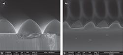
Patterning periodic structures on sapphire is carried out by ICP RIE with patterned PR mask on top of sapphire substrates. Creating accurate and uniform high-precision structures in the PR mask is the first step to making successful, effective PSS. Equally important is to subsequently maintain the structural integrity of this high-precision patterned PR mask through the ICP RIE process. This structural rigidity can be accomplished by hardening the resist and/or substrate cooling in an ICP RIE system. Fig. 3 shows how seriously the resulting PSS quality would be compromised if the resist structural integrity and precision were not properly sustained through the etching process.
Other key process considerations in the ICP RIE process that are critical to the PSS profile characteristics are sapphire etching selectivity against PR mask, bias RF power, ICP process pressure, RF coil design for plasma uniformity, plasma chemistry, and substrate temperature control. Success in accomplishing the most effective PSS fit for a target application is determined by how intelligently and meticulously all these parameters are combined and implemented. Fig. 4 demonstrates how drastically different patterns can be engineered depending on the way these parameters are put together.
PSS market trends today
Until now, the PSS industry has been driven predominantly by LED chipmakers. They either fabricate PSS in-house or outsource it to contract manufacturers. This trend is beginning to change, and dominance is shifting from LED chipmakers to sapphire substrate manufacturers.
Today, sapphire wafer manufacturers have begun to put patterns on sapphire wafers in partnership with the LED chip manufacturers. However, most sapphire manufacturers are concentrating on small diameter patterning in the 2-to-4-in. range. Only a small number of companies are beginning to introduce 6-in. products. Rubicon Technology launched larger-diameter PSS products in 4-, 6-, and 8-in. diameters in 2013 and differentiated their offerings with better control of quality and the most vertically integrated approach in the industry.
DONGGEUN KO is vice president, technology; JACOB YOON is development manager; and JANGHO SEO is senior development engineer at Rubicon Technology.


