UV and industrial LED applications require efficient thermal substrates (MAGAZINE)
A nanocrystalline aluminum oxide dielectric layer on LED module substrates provides the excellent thermal conductivity needed to ensure reliable operation of high-output sources in industrial applications, explains PEKKA KATILA.
There is a growing industrial market for high-power ultraviolet (UV)- and visible-light LEDs in curing, machine-vision, and other applications that require high-output sources. The application requirements for industrial high-power LED components and luminaires dictate that products must be of reasonable cost while guaranteeing high levels of reliability, ensuring long lifetimes and minimal or no maintenance downtime. These demands necessitate the development of modules that are both thermally efficient and protected from the immediate operating environment.
Let's briefly consider the applications. A key usage is in curing equipment used for drying paints, adhesives, and other curable materials. These applications can use both visible and UV light in a range of wavelengths below 450 nm, typically applying UV-A band wavelengths between 365-405 nm. For more background on UV LEDs and curing, see a recent feature article on the topic. Similar modules are also used in the visible spectrum for machine-vision applications that require high-intensity illumination with monochromatic and/or white light LEDs.
When in use, an LED chip will emit light and also produce excess heat. LED chip performance is negatively affected when used in excess of the optimal operating temperature, leading to a reduction in both light output and module lifetime. As a rule of thumb, LED lumen output drops 0.3-0.5% for each 1°C increase in temperature while operating within the typical operating temperature range.
In order to produce a stable and uniform output while maintaining high reliability, a reduced operating temperature is required. This is because lower operating temperatures are needed for the extraction of maximum optical efficiency and because a lower temperature is the key factor in achieving a stable color temperature and better color rendering. When proper operating temperatures are maintained, a module will benefit from the LED chips' intrinsic high efficiency and long lifetime.
Therefore, the objective for an LED module designer is to have the lowest possible thermal resistance, allowing for the excess heat to be dissipated away from the chip as fast as possible in order to maintain the optimal temperature. Providing the appropriate thermal design for modules and for system-level assembly is challenging due to the fact that chip-level powers are increasing and system architectures are evolving to become more complex. This necessitates new technologies to further improve thermal management.
Substrate options
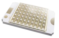
Chip-on-board (COB) based industrial modules are typically used in industrial applications (Fig. 1). These differ from COB LED arrays with a single large, circular light-emitting surface. Industrial COB modules can be rectangular in form and feature discrete LEDs. Both, however, share the concept of emitters attached to a thermal substrate.
The industrial modules range from a few watts up to 100W per COB, with COB areas up to around 10 cm2. Such modules are capable of delivering optical power density in excess of 10 W/cm2. Luminaires and larger illumination sources are generally assembled from blocks of these smaller COBs, rather than attempting to manufacture very large-size, extremely high-wattage COBs.
High thermal dissipation exceeding 20 W/cm2 as demanded by these COBs necessitates substrate structures capable of efficiently transferring the generated heat away from the active layer. Industry-standard substrates are usually metal core platforms such as metal-core printed circuit boards (MCPCBs) or more generally insulated metal substrates (IMS) sometimes known as metal-clad PCBs. For this class of substrates, aluminum and copper are the most common materials applied. These materials provide very high thermal conductivities of around 200 W/mK and 400 W/mK, respectively. However, these materials are electrically conductive and need an insulating dielectric layer.
TABLE 1. Comparison of common COB substrate materials.
Alumina | AlN | Silicon | MCPCB | Nanotherm | |
Mechanical strength (fragility) | X | X | X | • | • |
Thermal conductivity (W/mK) | X | • | • | X | • |
Cost of tooling | X | X | X | • | • |
Material cost | • | X | X | • | • |
Polycrystalline ceramic substrate materials are widely used for low- and mid-power modules. Alumina and aluminum nitride (AlN) materials, with thermal conductivities greater than 20 W/mK and 150 W/mK, respectively, are the most common ceramics in use.
Dielectric ceramic substrates, especially AlN, are an attractive choice for demanding applications as the conductor layer can be directly processed onto the material without the need for an isolation layer. However, the high cost of the material that results from its difficult manufacturing process and inherent fragility are preventing wider adoption.
TABLE 2. Characteristics of the UV-LED module.
Sample | P_tot (W) | P_opt (W) | Efficiency (%) | Thermal power, P_therm (W) | T_chip (°C) | Rth_total (K/W) | Optical power density |
1 | 74.8 | 25.4 | 34.0 | 49.4 | 54.6 | 0.60 | 7.5 |
2 | 74.8 | 25.3 | 33.9 | 49.4 | 52.9 | 0.56 | 7.5 |
3 | 74.8 | 25.6 | 34.2 | 49.2 | 53.6 | 0.58 | 7.5 |
4 | 74.8 | 25.4 | 34.0 | 49.3 | 55.7 | 0.62 | 7.5 |
Single crystalline silicon with high thermal conductivities exceeding 140 W/mK and low thermal expansion of 2.5 μm/mK makes an attractive substrate choice. For high-integration-level modules, silicon offers the option for monolithic integration of passive components and is a naturally convenient platform for hybrid integration of drivers. Also emerging gallium-nitride-on-silicon (GaN-on-Si) technology for processing white-light, blue-pump emitters directly onto silicon is further promoting that material as an attractive module-level substrate material.
To summarize, different substrate material compositions offer a variety of options for application-specific LED module designs, enabling them to reach better optical performance and lower cost. Table 1 provides a concise comparison of the options.
Nanotherm substrates
Now let's consider another emerging option. Nanotherm, from materials specialist Cambridge Nanotherm, is a novel substrate material for LED applications. Its unique construction offers the industry's highest thermal performance for a metal-clad PCB substrate. A nanoceramic process converts the surface of aluminum to form an extremely thin ceramic dielectric layer with best-in-class thermal conductivity. The nanoceramic dielectric thickness can be applied as thin as a 3-μm layer -many times thinner than conventional dielectrics. The combination of the thinnest dielectric layer in the industry with the highest conductivity yields the lowest thermal resistance of any material option.
This dielectric material has a nanocrystalline aluminum oxide layer that can be built to between 3 and 30 μm in thickness. The size of crystallites ranges between 30 and 60 nm. This size plays a critical role in giving the layer a unique combination of properties such as high thermal conductivity, high dielectric strength (around 50 V/μm), and flexibility (clearly visible when the nanoceramic is applied on foil substrates). The thickness of the dielectric layer can be tightly controlled to provide a close match to a product's breakdown voltage requirements. This avoids excessive dielectric thickness that unnecessarily increases the thermal resistance of the system. Nanotherm substrates offer thermal conductivity up to 152 W/mK, comparable to AlN.
In Fig. 2a and 2b you can see scanning electron microscope (SEM) images of the nanoceramic and anodic layers deposited on an aluminum substrate with through-holes (vias). The cross-section is made in the through-hole entrance area of each substrate. The figure shows a striking difference between the uniform density of the Nanotherm layer compared to the anodic layer, which has multiple cracks and delamination.
The ability to build a dense, uniform layer of ceramic on the surface of aluminum sets Nanotherm materials apart from other approaches. This creates the reliable dielectric properties that are required for electronics.
High-power UV COB design
Lumichip has manufactured a high-power UV COB-based LED module using a Nanotherm substrate to demonstrate the superior performance. The module construction has the following features:
• The substrate has an optimized dielectric layer thickness to allow the minimum necessary breakdown voltage strength while providing optimum thermal properties.
• The conductive tracks are made of plated copper.
• The layout is optimized for high reflectivity.
• Standard commercial materials are used with standard industry processes.
• The die-attach process is based on nanosilver material from Inkron instead of silver-filled adhesive. The silver sintering method is emerging as a new standard method for high-power LEDs. In this case we have applied a pressure-less process with a sintering temperature of 200°C to avoid degradation of the semiconductor chip.
• The wire bonding and mechanical protection with a silicone globe-top structure are made with typical materials.
The COB in Fig. 1 is a chainable 75W module with the LED array consisting of total 63 chips in a 7×9 format. The substrate thickness is 1 mm and it has laser-cut edges to achieve high dimensional accuracy for assembling modules into arbitrary length line sources. Total heat dissipation is about 50W and heat dissipation density is 20 W/cm2. With these thermal figures the optical output still exceeds 25W, yielding excellent efficiency of 34%.
Table 2 summarizes the module characteristics. The 75W LED module shows high efficiency close to 35%. Total optical output is greater than 20W at 385 nm. The module temperature is highly uniform with edge-to-center temperature difference being below 17°C.
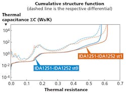
The nanosilver material provides superior thermal performance as shown in the T3Ster test graph (Fig. 3). The first step in the thermal resistance graph denotes the die and die-attach compound thermal resistance. The thermal impedance of die and bond-line material together is on average below 0.18 K/W.
Composite aluminum ceramic materials such as Nanotherm provide a cost-effective substrate material suitable for high-power LED modules, offering excellent mechanical and thermal characteristics. Lumichip has recently rolled out a full series of high-power LED COB modules for UV-A wavelengths 365 to 405 nm based on the Nanotherm platform.
PEKKA KATILA is director of integrated modules at Lumichip (lumichip.com).


