High-efficiency lighting needs high-efficiency manufacturing
Modern LED manufacturing facilities are very complex, and use large amounts of energy and materials both in construction and operation. Utilizing sophisticated planning and design tools, and considering “reduce, re-use, and recycle” options, such as the conversion of under-used older generation semiconductor facilities, projects can be completed faster, with minimized environmental impact, and with an improved bottom line. Don Carkner explains.
Manufacturing high-brightness LEDs is a complex process that requires a highly controlled environment, including sophisticated and highly customized equipment and facilities. It also requires the use of large amounts of energy and materials during both construction and operation.
Organizations approaching such a venture must not underestimate the scale of the challenge, or the importance of sophisticated advance planning. Done properly, these can help to achieve both high-performance operation and minimal environmental impact.
It is possible to plan, design, construct and operate complex LED facilities in a manner that is attractive both economically and environmentally, using proven methodologies refined over many years of project experience.
Reduce, Re-use, Recycle
REDUCE: Greenfield Design for Efficiency
Normally, LED manufacturing facilities are purpose-built on a new (“greenfield”) site. This allows the widest possible range of options for factory size and layout to be explored, and also allows the design-in of critical and highly integrated infrastructure. In these cases, a careful design approach will help to minimize costs and environmental impact from end to end of the project.
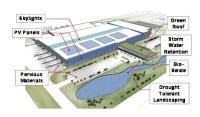
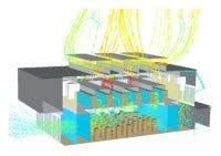
Some of the factors that can have a bearing on the facility’s energy and environmental footprint are illustrated in Figures 1 and 2. The incorporation of skylights, PV panels, green roofing and airflow modeling reduce lighting and heating or cooling costs. In the surrounding site, many other efficient design options exist that reduce water required for irrigation and prevent harmful runoff.
RE-USE: Brownfield options
An alternative to starting with a greenfield site is to start from an existing facility and modify it to suit the needs of LED manufacturing. This so-called “brownfield” strategy has become more attractive in recent years, due to market changes in the semiconductor industry.
The march of semiconductor technology to larger wafers and smaller feature sizes has created an assortment of older generation semiconductor fabs which are ripe for re-purposing for another type of manufacturing that requires similar infrastructure.
Analysis done by CH2M HILL indicates that a typical 200 mm wafer fab could be an attractive option for LED production. In addition to the obvious clean room and air handling synergy, many other commonalities could be useful, such as the systems for de-ionized and process chilled water, compressed clean dry air and house vacuum, process gases, and acid & solvent supply and waste.
Structure:
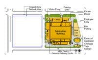
If we consider a generic 200 mm semiconductor fab, as shown in Figure 3, we can identify many aspects of the site that are common to LED production. Generally, the building has two to four stories, with a high level clean manufacturing space on the top floor, a lower level space on the bottom floor, and a cleanroom support space sandwiched in between. Surrounding the main facility is the supporting infrastructure, including a central utility building, gas supply and distribution for other process gases, bulk chemical storage and distribution, an electrical substation, parking and shipping/receiving areas and docks, and office spaces.
Each semiconductor fab is somewhat different, depending on the process and tools it was designed for, and so critical design constraints must be considered when evaluating a conversion project to LED. A comprehensive physical layout must be done before committing to move ahead.
Manufacturing support systems:
The most usable functional commonalities between a 200 mm semiconductor fab and an LED facility are the manufacturing support systems. In many cases, the LED requirement falls within the envelope of the capacity ranges of the existing systems. Care needs to be taken to remain within an efficient operating range, but with careful planning and design, many systems can be re-tuned to operate comfortably and efficiently in the modified facility.
A small number of systems would require augmentation, more extensive modifications or replacement. For systems that will be scaled-down or replaced in the conversion, there is an opportunity to recoup some cost by selling equipment on the global resale or salvage market.
Re-using time and money:
Another important factor to consider in a facility conversion project is the potential reduction in time to market that it may offer. A large cleanroom-based manufacturing facility project will require in the range of 25 weeks to construct the building before the actual cleanroom construction begins. This phase of the construction, including materials, will typically account for 30% of the overall cost. In a conversion project, these items are replaced by decommissioning and retrofit tasks, which should be much shorter in duration, and disposal costs, which are much less than the new materials. It is estimated that approximately 3 months and significant portion of the building cost can be shaved from the project vs. a greenfield construction.
In a recent project for a photovoltaic cell manufacturing client, CH2M HILL compared a new greenfield site with conversion of an older 200 mm semiconductor facility, and concluded that the overall capital cost savings for the facility exceeded 40%. In this specific case, capital cost was important to the start-up phase client, and so they were willing to compromise on some factors while gaining benefits such as substantial capital savings and room for future expansion. In any remodel situation, such give and take is important to produce a win-win result.
RECYCLE: Decommissioning options
In some cases, a new production facility is not the right solution. Sometimes it makes more economic sense to consolidate facilities, relocate a facility, or even decommission one. Even in these less-than-desirable situations, a properly executed environmental strategy can provide both tangible and intangible benefits for even the most challenging situations.
Rather than closing the original plant and constructing new one elsewhere, it may be preferable to relocate. This is the ultimate recycling option – essentially creating a brand new facility from an older one.
Conclusion
Reducing the environmental impact of operations has become part of the mission statement of companies worldwide. However, growing value and profitability is also vital to survival. The right approach and experience can help companies meet these goals with appropriate planning and the consideration of options following the “reduce, reuse, and recycle” mantra of modern environmental philosophy. Designing for increased efficiency, reusing existing manufacturing facilities, and environmental awareness at the end of a facility’s life are all examples of this methodology. In this way, the environmental impact of manufacturing growth can be minimized, and both upfront and operating costs can be reduced, creating a true win-win situation for the organization and the global community.
Further reading
- Andy Solberg and Steve Cook, “New Approaches to Energy-Saving Facility Design,” CleanRooms magazine, January 2009
- Terrence Morris and Steve Blaine, “Chiller Plant Optimization,” Semiconductor Fabtech magazine, December 2008
- Nate Monosoff, “PV Facilities: Opportunities for Conversion and Re-Use of Semiconductor Fabs,” Photovoltaics International magazine, December 2008
- Matthew Wilson, “Sustainability Strategies for Advanced Technology Facility Design,” 2008 Advanced Energy Conference sponsored by the Advanced Energy Research & Technology Center (AERTC), Hauppauge, New York, November 2008
- Ben Ighani, “Converting 200 mm Wafer Fabs to Flat Panel Manufacturing,” China International Display Conference (CIDC), Shenzhen, China; October 2008
- Converting 200 mm Wafer Fabs to PV Manufacturing, presentation by Ben Ighani to the PV Power Expo, Taipei, Taiwan; September 2008
- Andy Solberg, Dave Seger, and Michael Cowger, “Economizer Performance: Applying CFD Modeling to the Data Center's Exterior,” Tech Target magazine, SearchDataCenter.com; June 2008
- Andy Solberg, Dave Seger, and Michael Cowger, “Economize the Data Center: Programming & Airflow Modeling,” 7x24 Exchange Spring 08' Conference, Boca Raton, Florida; June 2008
- Scott Barton-Smith, Nick O’Neil and Gillard Tyson, “Critical Sustainability,” 2008 Oregon Design Conference; May 2008
- Nate Monosoff and Dick Sheehy, “Emerging and Growth Industries Zero In On Energy Availability & Costs,” Area Development magazine; April 2008
- Ben Ighani, “Trends in PV Manufacturing and Sustainability,” SEMICON China 2008, Shanghai, China; March 2008


