Conquering LED efficiency droop could lead to affordable LED lighting, says CLEO paper
May 4, 2012
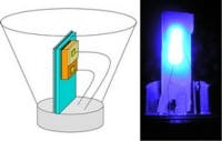
Date Announced: 04 May 2012 WASHINGTON -- Like a coffee enthusiast who struggles to get a buzz from that third cup of morning joe, light-emitting diodes (LEDs) seem to reach a point where more electricity no longer imparts the same kick and productivity levels-off. Now a team of researchers from California and Japan has devised a new design for green and blue LEDs that avoids much of this vexing efficiency droop. The findings will be presented at the Conference on Lasers and Electro-Optics (CLEO: 2012), taking place May 6-11 in San Jose, Calif.[Photo caption: Schematic of the transparent LED packaging design (left). A working blue LED using the design (right). Image courtesy Yuji Zhao, University of California Santa Barbara.]By changing the orientation of the crystal structure in semiconductor films, the team created LEDs with high efficiency and extremely low droop. Droop, which is a dramatic drop in efficiency at high currents, is one of the main problems limiting the growth of the solid-state lighting market.Blue and green LEDs provide the essential hues that blend with other wavelengths to give us the familiar white light we expect from household bulbs. These highly prized colors, however, have been among the hardest to engineer and the “droopiest” of the LEDs.“We believe this technology could be a big breakthrough and has the potential to change the future of lighting,” says Yuji Zhao, a graduate student at the Solid State Lighting and Energy Center at the University of California Santa Barbara (UCSB) and one of the lead researchers on the team.LEDs are many times more energy efficient than heat-spewing incandescent bulbs, but, due to droop, lose a significant fraction of that efficiency at the high current levels required for typical household lighting. No one is exactly sure what causes droop, although different research groups have offered several competing explanations. Despite the uncertainty, the UC Santa Barbara-based research team has developed a promising technique to minimize droop by making changes to the way the LEDs are manufactured. LED chips are made from layers of doped semiconductors sandwiched together. When a voltage is applied across the layers, electrons and holes (an absence of electrons) migrate toward an area of the LED called the active layer, where they combine, begetting a photon in the process. In most commercially available blue LEDs, the crystals that make up the semiconductor layers are grown in a flat orientation called the c-plane. This traditional orientation of the crystals, however, may create electrical fields that interfere with the reunion of the electrons and holes.The UCSB researchers’ LEDs have non-traditional, tilted crystal orientations that lessen the effect of the field, and exhibit some of the lowest reported measures of droop. Using this approach the team was also able to fabricate LED chips that are smaller than standard commercial LEDs, which could cut down on manufacturing costs. Further work remains to be done. “The biggest problem right now is the relatively high cost of the gallium nitride [GaN] bulk substrates,” says Zhao, referring to the thin sheets of crystalline material on which the group’s LEDs are grown. “At UCSB we are also developing methods to mass produce high quality GaN bulk substrates. I have confidence in this and I think it’s just a matter of time before [the cost of GaN] will no longer be an obstacle.”CLEO: 2012 presentation JTh4J.2, “Semipolar (2021) Blue and Green InGaN Light-Emitting Diodes,” by Yuji Zhao et al. is at 5 p.m. on Thursday, May 10 in the San Jose Convention Center.Press RegistrationA Press Room for credentialed press and analysts will be located on-site in the San Jose Convention Center, May 6 – May 11. Media interested in attending the conference should register on the CLEO website or contact Angela Stark at 202.416.1443, [email protected] CLEOWith a distinguished history as the industry's leading event on laser science, the Conference on Lasers and Electro-Optics (CLEO) is where laser technology was first introduced. CLEO unites the field of lasers and electro-optics by bringing together all aspects of laser technology, with content stemming from basic research to industry application. CLEO: Expo showcases the latest products and applications from more than 300 participating companies from around the world, providing hands-on demonstrations of the latest market innovations and applications. The Expo also offers valuable on-floor programming, including Market Focus and the Technology Transfer program.Sponsored by the American Physical Society's (APS) Laser Science Division, the Institute of Electronic Engineers (IEEE) Photonics Society and the Optical Society (OSA), CLEO provides the full range of critical developments in the field, showcasing the most significant milestones from laboratory to marketplace. With an unparalleled breadth and depth of coverage, CLEO connects all of the critical vertical markets in lasers and electro-optics. For more information, visit the conference's website at www.cleoconference.org.
Contact
Angela Stark CLEO: 2012 202.416.1433
E-mail:[email protected]
Web Site:www.cleoconference.org


