Today, the flat-panel display market primarily comprises liquid-crystal displays (LCDs) and organic light-emitting diode (OLED) displays targeting end products from large information and television displays to tablets, smartphones, and microdisplays for augmented and virtual reality (AR/VR) applications.
LCDs use an inorganic LED backlight to emit light through a matrix of liquid crystals to generate images. OLED displays are self-emissive, using organic compounds to emit light in response to an electric current.
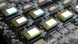
Emerging micro-LED display technology promises more color and higher brightness with lower power consumption than traditional displays. The first products have made an impressive entrance into the market, with TVs and video walls introduced by major display players promising the ultimate visual experience for entertainment, as well as business environments.
Micro LEDs are microscopic versions of traditional LEDs (>1 mm), measuring less than 50 µm. Whereas traditional LEDs are packaged individually, large numbers of micro LEDs are incorporated in bare die form to create displays. They are organized in subpixels, each containing red, green, and blue micro LEDs to form a color display. The emitted color is set by the bandgap of the inorganic material used to make the LED — e.g., aluminum gallium indium phosphide (AlGaInP) for red and indium gallium nitride (InGaN) for green.
Large modular display opportunity
A backplane transistor array, which switches and drives individual display pixels, controls an active-matrix micro LED display. Micro LEDs fall into two categories based on their backplane materials.
One uses silicon-based (Si-based) transistors, made with standard CMOS fabrication process flows. These transistors can be very small, resulting in backplanes with a high pixel pitch, which are ideal for high-resolution AR/VR applications or projectors. However, Si backplanes are relatively expensive, limited in size, and nontransparent.
A second category uses thin-film transistors (TFTs), made of amorphous Si, low-temperature polycrystalline Si (LTPS), or indium gallium zinc oxide (IGZO). TFTs can be processed on larger substrates than Si and have the potential to achieve a lower cost per unit area when processed in larger volumes. Micro LEDs on TFT substrates are the focus of this article.
One application is large, modular displays intended for TVs or video walls for the home, cinemas, advertising, or conference and meeting rooms. Depending on the size and number of modules, the final display can measure upwards of 200 in. In this application, micro LEDs on TFTs are expected to outperform OLEDs on TFTs because micro LEDs are more efficient, offering a higher luminance at the same drive current. Also, as there are no organic layers, micro LED displays do not require encapsulation, easing the way for a seamless transition from one module to another. With OLEDs, each module must be encapsulated separately.
Unlike OLEDs, micro LEDs intended for larger displays cannot be monolithically processed on the same substrate. Therefore, mid- to large-sized displays require other fabrication approaches, such as pick-and-place. In this approach, the micro LEDs are fabricated using three different epiwafers (for red, blue, and green), diced, and transferred onto a TFT backplane using a high-speed pick-and-place system.
Design considerations for micro LED TFT backplanes
High-performance micro LED displays introduce new challenges to backplane design. Different electronics approaches are being pursued — one starting from an active-matrix OLED (AMOLED) design approach, the other starting from a passive, PCB-based design.
Each method comes with pros and cons in terms of gray level, flickering, pixel pitch, heat dissipation, and power consumption. Imec is working to leverage its TFT circuit expertise into alternative pixel circuits that can advance micro LED displays. What follows is an example of a new TFT circuit design for modular micro LED displays, codeveloped with display/visualization technology provider Barco.
A 6T2C pixel circuit for driving micro LED displays
When developing a backplane circuit for a specific type of display, designers need to choose the optimal matrix architecture (active matrix driving versus passive matrix driving), the way the gray level is set (analog driving versus digital driving), and the LED programming mode (voltage versus current programming). Imec researchers have compared and assessed various state-of-the-art approaches to develop a hybrid method that combines the best of the different approaches in a novel 6T2C pixel circuit capable of tackling emerging challenges for micro LED displays.
Active versus passive matrix architectures
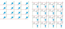
Both passive and active matrix displays use horizontal and vertical lines, respectively, to select a line and apply the corresponding image data to the columns to drive the pixels in that line. The lines are activated in high-frequency order, such that the human eye regards it as a planar frame rather than a line scan.
In passive matrix driving, used in today’s micro LED walls, pixels in the unselected lines are off. They turn on only for a short period when the line is selected. In other words, only one line is emitting light at the time.
In active matrix driving (comparable to in AMOLED designs), all pixels contain a storage element that allows them to remain active throughout the switching cycle until their values are updated again. Therefore, they also emit light when other lines are being programmed, reducing the pixel brightness requirement and current levels.
Active matrix designs offer benefits in power consumption, cost, and image quality. In passive matrix designs, pixels are only activated during a short period of time, requiring significantly higher peak brightness and corresponding current through the LEDs to achieve the same overall brightness. This increases power consumption and the need for heat dissipation. For large, modular displays containing millions of emitters, an active matrix driving scheme is therefore preferred over a passive matrix design.
Gray level: Digital or analog driving?
The amount of current flowing through an LED determines the gray level (or brightness) of the individual emitter. The gray level of each individual LED that composes a pixel contributes to the overall brightness of the micro LED display.
Panel-based designs used for AMOLED displays typically implement an analog driving technique: The analog voltage (or current) applied to the pixel results in a current through the OLED, determining the gray level. In this approach, a higher current level results in a higher light emission and thus a brighter pixel. But for inorganic micro LEDs, changing the current to vary the gray level also affects the wavelength of the emitted light, causing an undesirable color shift.
As a result, digital driving is preferred for a micro LED display. This approach uses pulse width modulation (PWM) to determine the amount of current flowing through the micro LED so a fixed current level is applied to every LED (without color shift). But the average time that the LED is on — or the duty cycle — can be varied to adjust the average light emission and thus the gray level of the pixel.
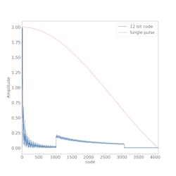
12-bit coding table
Multiple coding schemes exist for programming the PWM to implement digital driving. These coding tables contain the details of the exact time periods that the micro LEDs are on or off. Our R&D team has proposed a unique 12-bit coding table to achieve minimal dark time and optimized optical appearance, resulting in a strongly reduced display flicker.
6T2C pixel circuit
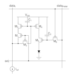
Designing the pixel circuit requires several choices to be made. For example, a designer can opt for a more traditional two-transistor–one-capacitor (2T1C) design, in which one transistor selects the pixel and another transistor drives the current through the LED by setting the incoming data voltage. However, any variations in transistor characteristics can result in current variations and color shifts, so a voltage driven approach should be avoided.
Researchers from imec and Barco have developed a hybrid approach in which a fixed current through the micro LED is accurately set by a so-called current mirror, defined by two transistors; and the PWM data are applied by voltage levels, enabled by two switching transistors. These switching transistors turn the fixed mirrored current on or off, following the coding table. The two remaining transistors of the 6T2C circuit select the pixel where the input current is updated.
By using this pixel circuit, the joint R&D team was able to implement the proposed hybrid design approach to drive the micro LED display with optimal performance. It has also proposed variations of the 6T2C pixel circuit to broaden its applicability — for example, a variation to reduce the overall area consumed by the pixel circuit, based on the concept of current mirror sharing, and a global shutter design to improve the synchronization with which the sub-modules of a modular display are refreshed.
Moving toward high-volume manufacturing of TFT backplanes
Innovative pixel circuit design enables high-performance, large-area micro LED displays while reducing the display fabrication costs. The proposed active TFT–based matrix design will lower fabrication costs when compared to active-matrix Si CMOS or hybrid Si CMOS/TFT backplane technologies because the TFT backplane design uses larger substrates (compared to Si) and expands the potential of producing the TFTs in large volumes. A unique foundry model with TFT manufacturers has been pioneered and set up, which is similar to the existing multiproject wafer services for Si CMOS technology.
To illustrate these manufacturing capabilities, the imec and Barco team has designed a micro LED prototype display with LPTS backplane, based on the described pixel circuit design, which is subsequently fabricated in a selected TFT foundry. LPTS was preferred over IGZO as the TFT material due to its ability to handle higher currents for driving displays.
Conclusion
A hybrid approach for designing micro LED TFT backplanes combines the best of existing approaches: a current programmed, PWM-driven active matrix design. A novel 6T2C pixel circuit facilitates the hybrid design approach to drive micro LEDs with optimal visual quality. When manufactured in high volumes, TFT backplanes for driving micro LEDs offer a lower-cost alternative while maintaining high performance compared to traditional passive PCB-based designs or to a pixel-embedded Si CMOS chip technique.
*Imec offers R&D, prototyping, and fabrication services such as those described in this article.
REFERENCE
The results described in this article were presented by Kris Myny on behalf of imec at the 21st International Meeting on Information Display (IMID 2021).
Get to know our expert
KRIS MYNY received his Ph.D. in electrical engineering from the KU Leuven, Leuven, Belgium, in 2013. He is now a principal scientist at imec and professor at KU Leuven. Myny specializes in circuit design for flexible thin-film transistor applications. His work has been published in numerous international journals and conferences, including Nature Electronics and several ISSCC contributions. He was listed as one of Belgium’s top tech pioneers by the business newspaper De Tijd and in 2018 received the European Young Researcher Award for design on thin-film electronics. In 2016, Myny also received a prestigious ERC Starting Grant from the European Commission to enable breakthrough research in thin-film transistor circuits (FLICs). He is now a member of the Young Academy of Belgium (2019–2024), while serving as track chair of the IEEE FLEPs and VLSID conferences and as a member of the editorial board of the new IEEE Journal on Flexible Electronics.
