MICRO LED MANUFACTURING | Are cubic InGaN, red micro LEDs on your roadmap?
Exploding interest in augmented reality (AR) and virtual reality (VR) applications has already triggered development activity in the markets for the key enabling hardware, components, and materials. The potential to deliver a cost-effective, head-mounted display with leading-edge user experience is central to success in AR/VR applications, so the acceleration of foundational technology investments in recent years is unsurprising.
Technologies under examination include liquid-crystal displays (LCDs), organic light-emitting diodes (OLEDs), and mini and micro LEDs. ResearchandMarkets' 2021 forecast suggests that the opportunity for micro LEDs driven by AR/VR applications could hit $21 billion by 2027 with a CAGR of 81%. Still, the market remains in its infancy and micro LEDs are currently confined to a few high-end applications.
Performance improvements from miniaturizing devices may be dwindling. A radical approach may be required — one that delivers advantages over existing device-level technology, but can also be dropped into existing manufacturing lines. If the micro LED approach can scale to a full commercial level, it offers the optimal combination of attributes for the AR/VR application. Anyone who manages to overcome the technology stumbling blocks in micro LEDs stands to control the AR/VR displays market.
This article examines a potential solution based on fabricating LEDs from the cubic form of gallium nitride (GaN) rather than the hexagonal phase typically used, with improvements in efficiency and performance of small-form color emitters.
Efficiency challenges of small-form LEDs
A primary pain point for micro LED display developers is the lower efficiency of small-form LEDs. First, a few definitions. A micro LED is an emitter smaller than 100 µm; a mini LED would between 100 and 300 µm; and conventional or large-area LEDs can vary from 300 to 1,000 µm in size.
Typical high-efficiency, large-area LEDs are usually constructed from two material systems. Blue and green emitters are generally produced using diode structures fabricated from multiple layers of hexagonal crystalline indium and gallium nitride (h-InGaN) alloys. The red devices are made from structures comprising multiple layers of cubic crystalline aluminum, indium, and gallium phosphide (AlInGaP) alloys.
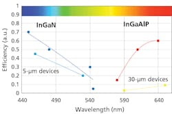
Larger-scale blue and red devices exhibit high internal efficiency — around 90% and 60%, respectively — while the efficiency for green emitters is approximately 20–30%. This efficiency deteriorates significantly when the size of the devices falls to around 5 µm: Blue emitter efficiency falls to about 40%, which is adequate, but that for green and red drops to a few percent at best. In fact, current state-of-the art, small-form red emitters deliver efficiencies of approximately 1–2%. These limitations are represented in Fig. 1.
Increased efficiency would improve configuration and would minimize concerns over power requirements for head-mounted displays. The amount of light emission required for a display to function properly will determine its battery size requirements and lifetime. Moreover, if significant energy is lost as heat, larger heat sinks will restrict form factor reductions of AR/VR displays. Therefore, addressing the loss of efficiency in small-form green and red LEDs would unlock the AR/VR opportunity for aspiring market participants.
Differences between micro LED manufacturing systems
For a full-color display, then red, green, and blue micro LEDs should be reasonably matched with respect to the spectral sensitivity of the human eye and have usable efficiency. There are two initial considerations:
- Select a material system and device design capable of delivering an LED with an acceptable underlying efficiency in the various regions of the spectrum.
- Understand and manage the impact of the device size reduction on that efficiency to produce the required small-form emitters.
Producing blue LEDs with very high efficiency is possible in the conventional h-InGaN material system. The size reduction impacts emitter efficiency, but with suitable mitigations, one can produce blue micro LEDs with workable efficiency — around 5–10% for early versions.
Physical effects that arise in the devices are driven by changes in material composition required to access longer wavelengths. The fundamental properties of the hexagonal crystal structure are also a contributing factor. While the h-InGaN system can, in principle, be engineered to produce emitters across the whole visible spectrum, more work is required to wring sufficient efficiency out of LEDs of all sizes fabricated via h-InGaN for longer visible wavelengths.
Turning to the AlInGaP system, producing highly efficient, large-scale red and amber LEDs in this material is possible. However, when the emission wavelength falls into the green region, the efficiency collapses due to fundamental physical limitations in material properties. For the same reason, coverage of the blue end of the spectrum is impossible. Although using two different material systems to address the range of colors required for a display is not ideal, the AlInGaP system does have potential for dealing with red devices. That said, in this material, managing the impact of size to produce small-form LEDs is a more difficult proposition than in the h-InGaN system.
While overcoming this challenge is possible, experience suggests that the high efficiency exhibited by large AlInGaP devices collapses to a few percent as the device shrinks. Again, the production of red micro LEDs based on AlInGaP remains a work in progress. Even if the efficiency challenges can be overcome, integrating different material systems into a single display is a suboptimal solution.
Current methods
Most of the work on micro LEDs has focused on h-InGaN since it has delivered rapid improvements in LED performance over its 30-year lifetime.
As mentioned earlier, the reasons behind the deterioration in h-InGaN LED efficiency at longer wavelengths are well understood by materials scientists and LED developers. A large, internal electric field arises from the asymmetry of the hexagonal crystal structure in certain directions. The field extends across the quantum wells (QWs) that form the active region of the LED, irrespective of device size. The electric field tends to separate the electrons and holes in the QWs and reduce the rate of radiative recombination, a process that is fundamental to the emission of light. This situation is exacerbated by increasing the indium content of the QWs, a necessity if longer wavelength emissions are desired, such as green, amber, and red. Worse still, these internal electric fields limit the width of the QWs that can be employed, further constraining the tools that device designers can use to access longer wavelengths.
Much of the work aimed at bypassing this roadblock has focused on trying to move the electric field into a direction that does not interfere with the radiative recombination process in the QWs by rotating the crystal structure with respect to the device. The structure is grown on a substrate with its surface cut parallel to a crystal plane at a significant angle to that usually employed for h-InGaN LED layers.
Unfortunately, while this rotation technique helps with the internal electric fields, it also results in the need to manage defects that appear in the grown layers, which generally do not appear in the traditional growth direction. Managing this trade-off is tricky and these approaches have yielded little more than a few incremental improvements in efficiency of green, amber, and red h-InGaN LEDs. A more fundamental change in approach is essential for a market breakthrough.
Is a cubic structure the answer?
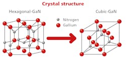
Materials scientists and LED developers have long understood that the InGaN alloys forming the basis of the LED structure can also crystallize in a cubic structure (c-InGaN). The structures are compared in Fig. 2.
The cubic structure offers potential benefits over the usual hexagonal crystalline form:
- The internal electric fields that cause the collapse in efficiency with increasing wavelength in h-InGaN LEDs are completely absent in c-InGaN due to the higher symmetry of the cubic structure. This makes the use of wider QWs to access longer wavelengths possible, something precluded in h-InGaN devices. It is also expected to reduce spectral drift with increased drive currents.
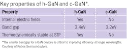
- The bandgap of c-GaN is 3.2eV compared to 3.4eV for h-GaN, meaning that the baseline emission from a device employing that material will be at a longer wavelength even before the addition of indium. So lower indium content will be required to access a given wavelength when compared with h-InGaN devices. The ability to employ wider QWs in this material system is a further benefit (see table).
- The hole mobility and maximum hole concentration achievable are materially higher in c-GaN than in h-GaN. The ability to produce highly conductive p-type layers is vital to successful LED operation at high current densities.
Until recently, the c-InGaN system has gone relatively unnoticed due to the rapid progress made in h-InGaN applications and historic difficulties around reliably producing, manufacturing, and scaling pure c-InGaN layers. With progress in h-InGaN reaching a plateau, interest in the cubic system has been rekindled.
Kubos Semiconductors, a spin-off from the University of Cambridge, in the U.K., has established a reliable and scalable manufacturing route for c-InGaN structures. It utilizes industry-standard metalorganic chemical vapor disposition (MOCVD) equipment and silicon substrates. Growth on 150-mm-diameter substrates has been demonstrated (see Fig. 3), and early results support the predicted promise of using c-InGaN to fabricate more efficient, longer-wavelength LEDs. This in turn raises the prospect of producing red, green, and blue micro LEDs from one material system and in the same MOCVD reactor. In doing so, it provides a roadmap to monolithic c-InGaN RGB pixel arrays.
Although work remains to optimize QW emission efficiency, compelling evidence exists supporting the consideration of a cubic InGaN system to produce LEDs with adequate underlying efficiency in the green, amber, and red parts of the spectrum. Furthermore, if the robustness of h-InGaN LEDs to the reduction in device area can be maintained in the cubic form, this material could be the breakthrough for red micro LEDs that unlocks the AR/VR display market.
The author represents Kubos Semiconductors, which has established a fabrication technique for LEDs as described in this article.
Based in Milton Keynes, U.K., MARTIN LAMB is chairman of Kubos Semiconductors. He has 40 years’ experience in the compound semiconductor materials industry, holding senior positions including managing director of Wafer Technology Ltd. Lamb was part of the team that effected a management buyout of Wafer Technology in 1994, turning the business profitable and winning the Queen’s Award for Export in 1997. The company was then sold to IQE plc, where he served on the main board. Since leaving IQE plc, Lamb has been active as a business angel, investing in 12 early-stage companies in the technology sector. He serves on the boards of several companies within his portfolio. Lamb holds a BSc in applied physics and electronics from Durham University and an MBA from the University of Leicester, both in the U.K.
Follow our LinkedIn page for our latest news updates, contributed articles, and commentary, and our Facebook page for events announcements and more. You can also find us on Twitter.


